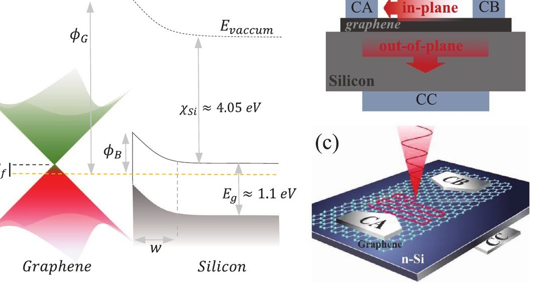
Electrons in an atom-thin sheet barely move out of the sheet, so the uncertainty principle links a 2D layer's thickness to how easily charge enters the material beneath it. We stacked uncoupled CVD graphene layers one by one on silicon to test this on a macroscopic device.
In-plane current scales with the number of assembled layers.
Layer thickness strongly modifies charge injection and the reverse saturation current of the graphene–silicon junction.
Cite
M. Javadi, A. A. Noroozi, A. Mazaheri, Y. Abdi, "Sequentially assembled graphene layers on silicon, the role of uncertainty principles in graphene–silicon Schottky junctions," Advanced Optical Materials 7, 1900470 (2019). https://doi.org/10.1002/adom.201900470